Introduction:
Transistors have 2 different applications; they are used as:
- Amplifier (think of an audio amplifier)
- Switch (a transistor can switch large powers very quickly and is used in control units in cars, among others).
Transistors are controlled with current. In microprocessors, for example, the current is kept as low as possible to avoid heat development. The MOSFET is often used in this case.
There are two types of transistors, namely the NPN and PNP transistor. These are described below.
NPN transistor:
The B stands for “Base”, the C for “Collector” and the E for “Emitter”,
In the NPN transistor, the arrow of the transistor is directed away. This transistor is often used when it is a ‘ground switching’ arrangement, with the Emitter connected to ground.

PNP transistor:
In the PNP transistor, the arrow is directed towards the transistor. A handy mnemonic for PNP is also “Pointing towards Plate”.

Operation of the transistor:
In automotive technology, the transistor is most often used as a switch, so we will focus on that now. We will use an NPN transistor as an example.
In the illustration, the base is on the left, the collector is above, and the Emitter is below. When a base current flows (blue arrow), it finds its way to the Emitter. This also causes a collector current to flow to the Emitter. As soon as the base current stops, the current from collector to Emitter also stops.
If a half base current flows, then a half current (compared to I max.) flows as well. It is clear that the current switched by the transistor (from C to E) is entirely dependent on the amount of B.
A transistor always has voltage losses due to the PN junction. Between the Base and Emitter, it is 0.7 Volts, and between the Collector and the Emitter, it is 0.3 Volts.
The transistor as a switch:
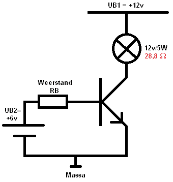
In the following example, a lamp of 12 volts / 5 Watts is controlled with a transistor. The voltage of UB1 (voltage source 1) is the battery voltage of 12 volts. The lamp is ground-switched. The base of the transistor is controlled with UB2; “voltage source 2” of 6 volts.
The voltage drop between Collector and Emitter (UCE) is 0.3 volts, and between Base and Emitter (UBE) is 0.7 volts. We will see this return in the calculation below. The amplification factor is determined to be 200. This can always vary. The amplification factor is the ratio between the base current and the Collector-Emitter current.
A circuit must always be executed with a certain resistance (in the above schema RB). If this resistance was not present, the transistor would be damaged immediately. The value that the resistance RB must have depends on all factors; namely, voltages on both UB1 and UB2 and the required current for the components (resistors or lamps), etc. We will now calculate the load resistance RB.
To calculate the load resistance RB, the resistance through the lamp must first be calculated.
Now that the resistance RL is known, the collector current (IC) can be calculated.
UCEsat stands for “saturation,” meaning saturation. As soon as the transistor is conductive, a voltage loss of 0.3 volts arises between points C and E (Collector – Emitter).
The next step is to determine the base current (IB):
In every transistor circuit, a safety margin (IBK) of 1.5 x IB applies. So the value of IB must be multiplied by 1.5 again. The reason for this will be explained later.
The base current is only 12% of the Collector-Emitter current. Now it is clear that a transistor can make a large main current from a small base current.
Now that all currents in the circuit are known, the resistance RB can be calculated.
UBE is the voltage between the Base and the Emitter. Due to the conductive material in the transistor, there is always a voltage loss of 0.7 Volts between points B and E.
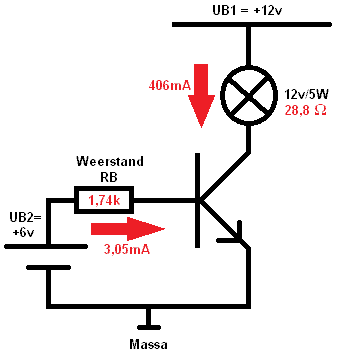
There are no standard resistors that are exactly 1.74k (Kilo-Ohm). So a standard resistor with a different value must be chosen. The choice must be made from the available resistors in the E12 series.

The required resistance of 1.74k is between 1.5k and 1.8k. In that case, the lower resistance value should be chosen; 1.5k. This is to ensure that aging and wear of the components do not affect the currents in the circuit.
The transistor as an amplifier:
The transistor can be used as an amplifier. The base current can be changed by turning a potentiometer. By varying the base current, the amplification voltage and thus the voltage across the collector-emitter changes.
Transistor characteristics:
A characteristic of an NPN transistor can be made, see the image below:
1st quadrant (top right) = UCE – IC
Up to 0.3 volts, the line runs diagonally upwards. This area is UCEsat (saturation of the transistor). After that, the line runs almost horizontally.
2nd quadrant (top left) = IB – IC
Here, the relationship between UB and IC is indicated. IC = HFE x IB, with HFE= 10 in these characteristics, so IC is 10 times as large as IB. The safety factor of IB = 1.5 x IBK has not yet been included here.
3rd quadrant (bottom left) = UBE – IB
The voltage loss between the base and Emitter of a transistor is the threshold voltage of a diode. The threshold voltage is 0.7 Volts. From this voltage, the transistor begins to conduct and the base current IB flows. This can also be traced back in the characteristics.
Example circuit with characteristics:
Now it’s time for a (simple) example circuit with an associated transistor characteristic. Here, the IB = 1.5 x IBK is included, resulting in a horizontal line on the IB axis. In the circuit below, UB1 is the battery voltage and UBE (voltage Base-Emitter) comes from a switch or signal in a control device. To calculate the current on UBE, the collector current (IC) must first be calculated;
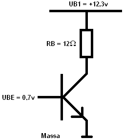
We now know that a current of 15mA must run on the base of the transistor to make the transistor (with the mentioned UB1 and RB) fully conductive, including the safety factor. Then the characteristics can be filled in:
In these characteristics, it can be seen that the IB (current on the base) increases to 10mA. This part, from 0 to 10 mA, is calculated with the formula: IB = IC : HFE. Then the line runs completely horizontal from 10 to 15mA. This part is the amplification factor of 1.5 (from the calculation of IB = 1.5 x IBK). At a base current of 15mA, there is a collector current (IC) of 1000mA.
Transistors are controlled with current. In microprocessors, for example, the current strength is kept as low as possible to prevent heat development. The MOSFET is often used in this context.
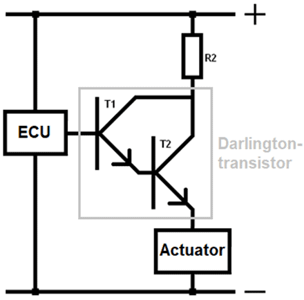
Darlington transistor:
A control device sends a base current to the transistor. A transistor can be made conductive by a control device with a current of 0.1 to 0.5 mA. When we want to control an actuator that requires a high current, the ECU cannot provide the necessary current for the transistor. The primary current of a coil is approximately 8 Amperes. The control current will have to be amplified to make the transistor conductive. This poses a problem: the microprocessor cannot provide the desired current for the transistor.
By means of a Darlington transistor, a large current can be switched to the actuator with a small control current from the ECU.
The Darlington transistor is composed of two transistors connected together in one housing.
The collector-emitter current of T1 provides the base current of T2. This results in a high amplification factor, as the amplification factors of both transistors can be multiplied.
A very small base current of T1 (just a tenth of a milliampere) is often enough to make T2 conductive.
The current amplification factor (Hfed) of the Darlington transistor is often between 1000 and 10,000. The formula to calculate the amplification factor of a Darlington transistor is:
Hfed = Hfe1 * Hfe2
- Advantage: thanks to the large current amplification factor (Hfed), a small control current is enough to make the Darlington transistor conductive;
- Disadvantage: The base-emitter voltage of the Darlington arrangement is twice as large as with a single transistor. The voltage loss of the Darlington transistor is therefore significantly larger than that of a single transistor.
In the paragraph “Output signals” on the page Interface circuits examples and applications of the Darlington transistor are mentioned.
Related page: