Subjects:
- Preface
- Transistor Transistor Logic (TTL)
- Conversion of analog sensor voltages to digital message
- Conversion of encoder signal to digital message
- Output signals
Preface:
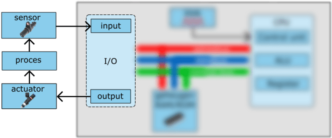
In most cases, the electrical signals coming from the sensors must be modified before being presented to the processor. The actuators are controlled on the other side of the computer. These are often inductive circuits that often switch large currents. The hardware to adjust the sensor signals and actuator currents is called interface circuitry. An interface circuit ensures the translation of an analog to a digital voltage.
- Sensors transmit a voltage with a low current. The interface circuit converts the voltage into a digital value (0 or 1).
The current is low with a sensor signal; - Actuators require higher current.
Around the control actuators, are located in the ECU in the form of (a combination of) transistors or FETs, which are also called “drivers”. We will discuss this in more detail in the “output signals” section.
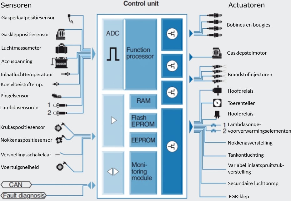
The image below shows the sensors and actuators of a (petrol) engine management system. The top group of sensors (from the accelerator pedal position sensor to the lambda sensors) fall under the “analog” category. This means that the incoming sensor voltages must first be digitized in the ADC (analog – digital converter). The lower group of sensors (the crankshaft position sensor to the vehicle speed sensor) already offer their signal digitally. The on-off signals or square voltages are applied directly to the CPU.
The actuators on the right side are controlled by an output stage. An output stage, also called a driver, consists of a circuit of several transistors to generate a usable voltage and current from a drive pulse from the computer to drive the actuator.
Transistor Transistor Logic (TTL):
The processor works with voltages of 5 volts. Input and output voltages are thus limited to a range of 0 to 5 volts (TTL level, abbreviated from Transistor Transistor Logic). For signals that deviate from this voltage level, an adjustment takes place in an interface circuit.
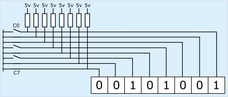
The images below show how a 1 or a 0 is formed from a switch position. By means of a pull-up resistor, the voltage of 5 volts creates a logical 1 on the input of the processor when the switch is open. The voltage across the pull-up resistor is then not connected to ground.
The moment the switches close, a voltage drop occurs across the pull-up resistor. The voltage of 0 volts on the input of the processor is seen as logical 0.
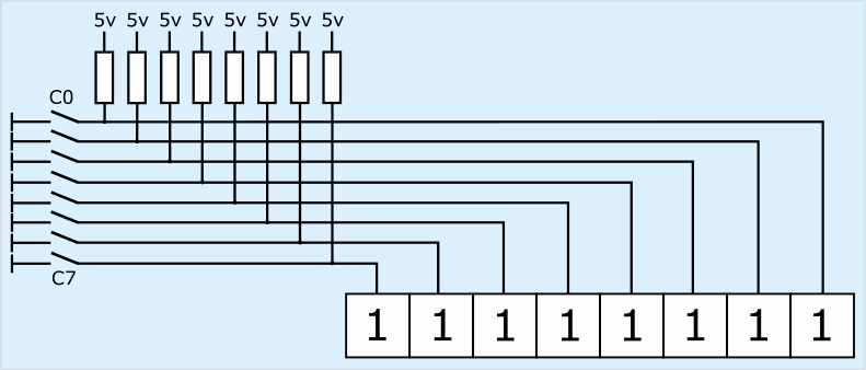
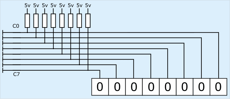
A combination of open and closed switches produces a sequence of ones and zeros. In the picture, the 8-bit message to the processor is: 00101001.
With an 8-bit processor, the eight bits per cycle are read simultaneously. During the next cycle, which occurs during the next “tick” of the clock (see the system bus on the ECU operation page) a sequence of eight new bits follows.
Conversion of analog sensor voltages to digital message:
Digital input signals are processed directly by the processor. Analog signals are first converted into a digital signal in the A/D converter. As an example we take the analog voltage curve of a turbo pressure sensor:
- steady state the voltage is about 1,8 volts;
- when accelerating, the voltage rises to almost 3 volts.
The voltage change cannot be processed directly in the processor. First, the measured voltage must be converted to a decimal value (0 to 255).
With a range of 0 to 5 volts and a decimal value of 0 to 255 (so 256 possibilities). A simple calculation shows that when we divide 5 volts over 256 possibilities, steps of 19,5 mV (0,0195 volts) can be made.
The above example showed the voltage curve versus time of a turbo pressure sensor. The voltage profile of a temperature sensor and accelerator pedal position sensor are similar, only in a different time frame: after all, heating up the coolant takes longer than spooling up the turbo.
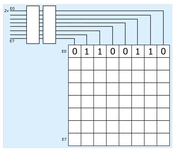
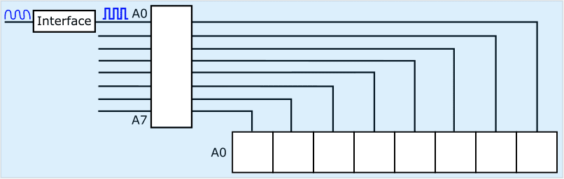
Earlier in this section there is an illustration showing a category of analog signals. This includes the temperature sensor and accelerator pedal position sensor. The analog voltage is converted into an 8-bit unit of information in the A/D converter. Many processors with multiple input pins have only one A/D converter. Multiple analog signals are combined into one signal by means of multiplexing.
In this example we see an A/D converter with eight inputs. Pin 0 has a voltage of 2 volts. Pins E1 to E7 can be supplied with voltages at the same time. These are converted one by one into a digital message by means of multiplexing.
The voltage of 2 volts is converted to a binary value. With the following formula, we can convert the analog voltage to a decimal value, and then convert it to a binary value:
2v / 5v * 255d = 102d
Here we divide the input voltage (2v) by the maximum voltage (5v) and multiply this by the maximum decimal value (255).
By means of a calculation or performing a handy trick, we can convert the decimal number of 255d to the binary value of 01100110.
See the page for this: binary, decimal, hexadecimal.
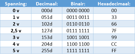
The following table lists the decimal, binary, and hexadecimal values associated with different voltages.
When reading live data, it is possible that the decimal, binary or hexadecimal value of the sensor signal is displayed.
- A voltage signal of <0,5 volts (025d) is considered a short to ground;
- If the signal rises above 4,5 volts (220d), the computer translates this as a short circuit with plus.
Conversion of encoder signals into a digital message:
The signals from pulse generators, including the inductive crankshaft position sensor, are actually on-off signals created after the teeth of the pulse wheel have moved past the sensor. The alternating voltage of the sensor must first be converted to a square-wave voltage before the signal is presented to the processor.
In the picture we see a sinusoidal alternating voltages on the left side of the interface. In the interface electronics, this alternating voltage is converted into a square-wave voltage. This block voltage is then read by the timer/counter block: the moment the pulse is high, the counter starts counting, and stops counting when the pulse becomes high again. The number of beats (counts) is a measure for the period time or. frequency of the signal.
In the image below we see a signal from the inductive crankshaft sensor with red dots in the upper flanks. The red dots are set to a voltage to increase (logic 1) or decrease (logic 0) the square-wave voltage. The explanation continues below this image.
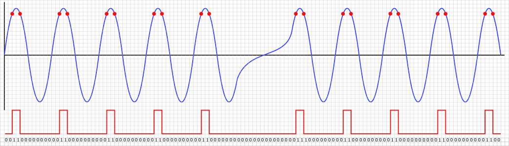
However, the sensor voltage is never completely pure. There will always be a small fluctuation in the voltage course. In that case, the interface electronics may incorrectly indicate this as a logic 0, when it should actually be a 1.
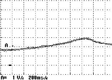
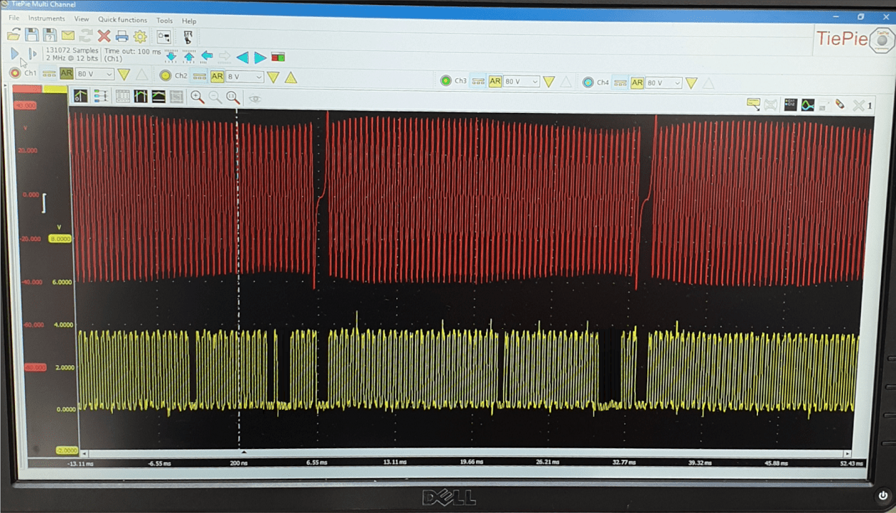
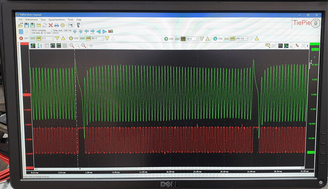
The scope image below was captured while performing the BMW Megasquirt project. The scope image shows the digitization (yellow) of the inductive crankshaft signal (red). The image clearly shows that pulses in the yellow block signal are missing, while at that moment no missing tooth in the crankshaft signal passes.
A so-called hysteresis has been built in to ensure that small fluctuations in the voltage profile do not lead to an incorrect interpretation of the ECU. The hysteresis is the difference voltage between the rising and falling edges of the voltage curve. In the image below we see that the red dots on the rising edges are at a higher voltage than the red dots on the falling edges. This way we know for sure that small fluctuations in the signal do not affect the digital conversion.
In the first section where we started about the conversion of the pulse signal to the digital signal, it was already mentioned that the frequency of the signal is determined on the basis of the time between two rising edges of the square signal. In these examples it is easy to deduce that the hysteresis does influence the width of the block signal, but has no influence on the time between the rising edges, and thus also has no influence on the frequency of the signal.
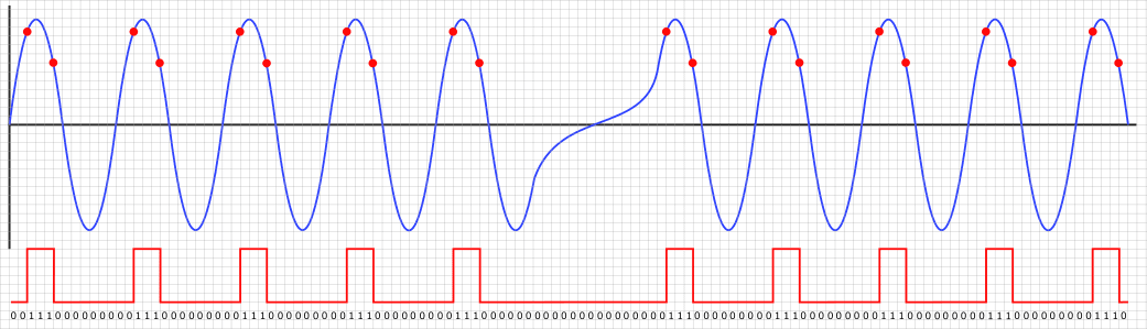
With a properly set hysteresis, the sinusoidal signal is properly converted to a usable square-wave voltage, with only the multiple logical ones in the places where the missing tooth passes.
Please note, during the setup of the MegaSquirt ECU, settings have been changed, including triggering on the rising and falling line. As a result, when passing the missing tooth in the first example the voltage is 0 volts and in the scope image below the voltage is 5 volts.
Output signals:
The output signals consist of digital on/off pulses with a voltage range between 0 and 5 volts (TTL level) with a very low current. Actuators, however, require driving with higher voltage levels and currents.
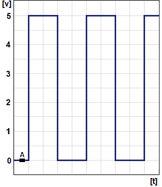
The on/off signals can be pulse width modulated (PWM), where the pulse width can vary at a constant frequency.
The following figure shows a square-wave voltage at TTL level as a function of time. The duty cycle of this PWM signal is 50%.
Drivers are required to control actuators. With the digital output signal, the required current can be achieved with a driver. In the next section we will discuss the drivers.
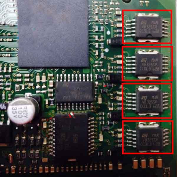
We find drivers in every ECU and in some actuators such as DIS ignition coils. We also call a driver an output stage or power transistor. The driver makes it possible to convert output signals at TTL level: 0 to 5 volts, with a low current of 1 mA from the ECU to voltages up to 14 volts and currents up to approx. 10 A.
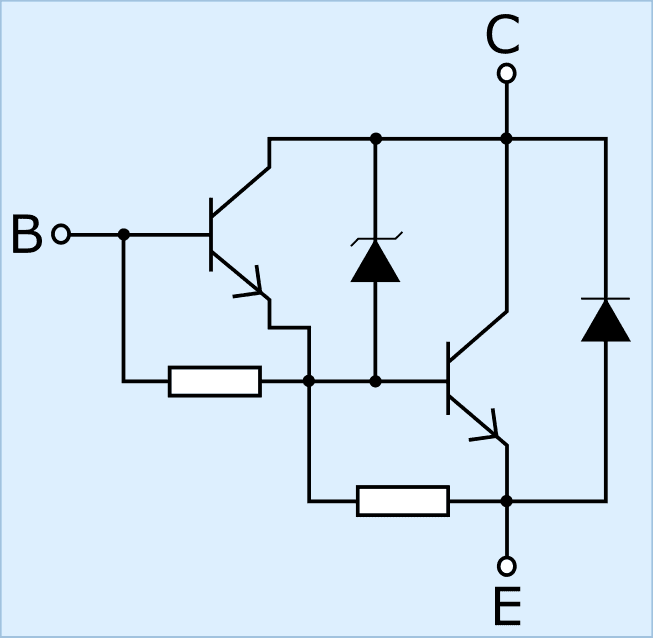
A driver can have several connected together transistors contain. We call such a transistor a “Darlington transistor“. The following images show the following circuits:
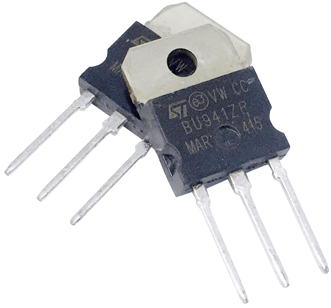
- Schematic of a darlington circuit with two transistors for the ignition coil drive (source: datasheet BU941ZR).
- Two transistors each with a darlington circuit (BU941ZR)
- Driver ICs with darlington circuits and additional electronics for temperature protection and feedback to the microprocessor.
On the page: control methods of actuators the control of passive, active and intelligent actuators by means of a (power) transistor or FET is discussed in more detail.